
| 8051 + LCD + EPROM |
| 8051 + LCD + EPROM |
Last Update March 30th 2004
 |
Several
other variations can be done. If using a 8051 derivative with internal
code memory as 8751 or the reduced pin count as 80C751 80C752 AT89Cx051
or other, the LCD can be attached to the same pinouts as show here.
A
variant of only 4 data pins can be implemented saving 4 port pins, this
is described at the end of this chapter.
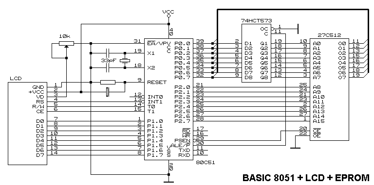
The variable resistor connected at LCD pin 3 (VD) and ground, controls the LCD display contrast. LCD's with extended temperature range (negative °C) can need a negative voltage at the VD pin (3), so the variable resistor need to be connected in a different way - the center tap goes to pin 3 (VD), one side to +5Vdc, while the other goes to a negative voltage around -3Vdc or more. To reduce power consume over this trimpot, you can try values higher than 10k ohms. I observed several LCD's that connecting VD to Ground is enough to result in a good display contrast. When you apply a resistor or a variable resistor to VD, a small current flows trough and a voltage develops over the resistor, normally this voltage is small between zero and 1 Volt.
The crystal connected at 8051 pins 18 and 19 needs the capacitors (33pF) connected to ground. Several 8051 works well without the capacitors, but some of them have intermitent clock "no-start" or "stop oscilattion" problems. To avoid problems just install the capacitors.
The 8051 reset pin receives a resistor (8k2 ohms) to ground and an electrolitic capacitor (10uF) connected to VCC. At power up, the capacitor is discharged, so current flows from ground to +Vcc via the resistor and the capacitor, until it charges the capacitor. This time can be calculated as aprox; time = 1 / RxC or 82milliseconds. The CMOS versions doesn't need the 8k2 resistor, but the books say it doesn't harm to install it. If you want to install a "reset" button, just install the switch in parallel to the capacitor, so when pressing the key it will apply +Vcc to the Reset pin, also discharging the capacitor.
The 8051 uses the Port P0 in some different ways when addressing external memory;
Reading EPROM
When reading the code memory, in this case an eprom, the 8051 breaks the 16 bits address (64k) into two bytes of 8 bits each. The high order bits are posted at the port P2 bits, while the low order 8 bits are posted at port P0 bits.
The 8051 then pulses up the pin ALE (30) to signal the external circuits that the address is available at the output of P0 and P2. This ALE up pulse tells the 74HCT573 (8 bits latch) to store the 8 low order address bits from P0. The output of this latch goes directly to the eprom low 8 bits address, and stays there until a new ALE pulse tells it to store a different address. At this point the eprom has the 16 address bits stable until P2 changes or ALE pulses up with a different value at P0.
The 8051 then pulses down PSEN pin 29 to get the program byte stored at the eprom, addressed by the above sequence. This PSEN low level pulse goes directly into the /CE eprom pin 20, this selects the eprom chip. The /OE (output enable pin 22) allows the eprom to outputs the byte addressed at pins 11-19. At this moment the 8051 reads the port P0 pins, and it will be the eprom output byte.
While no software instruction changes the P2 value, and the external eprom address 8 bits high order still the same, the P2 value will remains unchanged.
The
8051 reads external code memory whenever the EA (pin 31) is connected to
ground, even If the 8051 has internal eprom/rom.
To
execute the code stored into the internal eprom/rom (if exist) the
EA pin must be connected to +5Vdc (high level).
Years ago I build an emulator that uses a 8751 with internal eprom programmed to download data from a PC serial port at high speed and store it in an external RAM memory. This data in real was a 8051 program under development, to be executed by the 8051. After the data transfer, a manual switch side A changes the EA level from high to low and side B transfers the /CE RAM pin from the "external address decoding" to 8051 PSEN, so the 8051 "thinks" the RAM is an Eprom, and a new RESET makes the 8051 runs the downloaded program. It worked pretty well until I bought an EPROM EMULATOR, which is a much better tool.
The eprom at this example is a 27C512, so 64kbytes. Any other smaller eprom can be connected to this example, for sure reducing the high address bits. A 27C256 addresses only 32k and has only 15 address pins, A15 not used, 27C128 doesn't use A15 neighter A14, and so on.
External RAM is not shown in the drawing, but it can be connected exactly as the Eprom, pratically in parallel with the eprom, sharing the same 74HCT573 output, except pins /CE, /OE and /W. In this case, the /CE RAM pin is not connected to PSEN (PSEN means only reading instruction code), instead it is connected to an "external address decoding circuit" that activates low level whenever the 8051 drives /RD or /WR (pins 17 or 16) low meaning READ from or WRITE to the external RAM chip.
To write into the RAM, the 8051 post the high order address 8 bits at P2, the low order address 8 bits at P0, pulses up ALE to store P0 at the latches, then post the data to be writen at P0 and pulses /WR low. This /WR low need to be translated by the "external address decoding circuit" into --/W+/OE and --/CE to the RAM, this stores the byte from P0 into the RAM addressed by P2 and the output of the 74HCT573.
Toread from the RAM, the 8051 does the same addressing, but now it only pulses low the /RD pin, and the "external address decoding circuit" translates it into +/W--/OE and --/CE to the RAM, this reads the RAM and its contents is posted at the RAM output, so the 8051 reads this byte available at port P0 input pins.
|
|
|
In/Out |
|
|
|
Ground | - | Power supply zero Volts and Signal Ground. |
|
|
VSS | + | +5Vdc power supply. Works with lower voltages. |
|
|
VD
|
In | As described before, it needs to be close to ground level, and it can be adjusted via a variable resistor, trimpot or potentiometer, for a better view. Some extended temperature range LCD's may require a negative value at this pin. |
|
|
RS | In | Data sent to LCD can be a Character to be displayed (RS:High) or a command (instruction) to be executed by the LCD controller (RS:Low). |
| 5 | RW | In | Data direction. HIGH means Read from LCD, LOW means Write to LCD. |
| 6 | E or CE | In | CE:High tells LCD to initiate internal operation based on the RS, RW and Data signal levels. |
| 7-14 | Data pins (8) | I/O | Data to be displayed or command (Instruction) to be executed. |
Suppose our assembler code has the following equates:
RS bit
INT1
RW bit
T0
CE bit
T1
Busy bit P1.7
or
RS bit
0B3h
RW bit
0B5h
CE bit
0B4h
Busy bit 097h
Data
Write
To
write a character (Data) INTO the LCD display, it is necessary to
preset RS High, R/W low, character byte at Data Pins 7-14, and then pulse
CE pin up once.
Suppose we have the Data to write at the LCD at the accumulator, so the routine DataWrite would be:
DataWrite:
Mov
P1,A ; Post Accumulator at LCD data input
Setb
RS ; Set RS high (Data)
Clr
RW ; Set RW low (Write)
Nop
; Wait circuit settling
Setb
CE ; Tells the LCD to work (receive data
byte)
Nop
; Wait a little bit
Nop
;
Clr
CE ; Drop the selection line
Ret
; Return to Caller
Instruction
Write
To
write a command or address (Instruction) to the LCD, preset RS Low, R/W
low, command or address at Data Pins 7-14, and then pulse CE pin up once.
Suppose we have an instruction at the accumulator, to send it to LCD it
would be:
CmdWrite:
Mov
P1,A ; Post Accumulator at LCD data input
Clr
RS ; Set RS low (Instruction)
Clr
RW ; Set RW low (Write)
Nop
; Wait circuit settling
Setb
CE ; Tells the LCD to work (receive instruction
byte)
Nop
; Wait a little bit
Nop
;
Clr
CE ; Drop the selection line
Ret
; Return to Caller
LCDs with a chip on the back identified as HD44780 (Hitachi), HD44100H (Hitachi), M5259 (OKI) or SED1300F or others, understand a popular "standard LCD command set". We will describe it later.
The
most popular LCD displays are produced in 1, 2 or 4 lines, with 8, 16,
20 or 40 characters per line in this formats:
1x8,
2x8, 1x16, 2x16, 4x20 or 2x40.
At
power on, the LCD needs to be programmed for proper operation. It
consists to send a series of command bytes to the LCD.
For
our tests here, the sequence is 038h 038h 006h, 00Eh, 001h. This
will program the LCD for display active, new characters to the right, character
normal size 5x7 dots, increment cursor position, cursor on, not blinking.
(The initialization sequence map for 8 and 4 bits, you can find at the end of this document).
To do that, we just need to post those bytes one by one at port P1 (according with the drawing), and execute the Instruction Write as described above, for each byte in the sequence. Our assembler initialization routine would be:
LCDInitialize:
Mov
A,#038h ; Data
Lenght (8 bits), 2 lines, char 5x7
Call
CmdWrite ; Needs
3 times this byte (1st)
Call
Delay10ms ; Some delay
routine 10 milliseconds
;
Call
CmdWrite ; (second)
Call
Delay10ms ; Some delay
routine 10 milliseconds
;
Call
CmdWrite ; (third)
Call
Delay10ms ; Some delay
routine 10 milliseconds
;
Mov
A,#006h ; Move
direction and Shift Display
Call
CmdWrite ;
Call
Delay10ms ; Some delay
routine 10 milliseconds
;
Mov
A,#00Eh ; Display
and Cursor On, not blinking
Call
CmdWrite ;
;
Mov
A,#001h ; LCD
Clear
Jmp
CmdWrite ; ... and
return to caller
The Call Delay10ms instructions are necessary because the LCD needs some time to execute the first command sent, and the busy bit (explained later) is not working yet.
Now our LCD is ready to receive the first data, so the following instruction will write "HELLO" at the display;
Hello:
Mov
A,#'H' ;
Call
DataWrite ;
Mov
A,#'E' ;
Call
DataWrite ;
Mov
A,#'L' ;
Call
DataWrite ;
Mov
A,#'L' ;
Call
DataWrite ;
Mov
A,#'O' ;
Jmp
DataWrite ; ... and return to
caller
This data "HELLO" will be at the left of the first line. This is because it is following the "CLEAR" command send by the initialization routine. The instruction 001h is a clear command, it clears the display positioning the cursor at the left of the first line.
The
first left position of the first
line has the address 080h, the second 081h, third 082h...
The
first left position of the second
line has the address 0C0h, the second 0C1h, third 0C2h...
So, if you want to write the text "HELLO" at the second line instead the first, you need to send the address (Instruction) 0C0h to the LCD before you send the data bytes, so it would be;
Mov
A,#0C0h ; Position
cursor at second line left
Call
CmdWrite ; Tell Lcd to
do it
Jmp
Hello
; ... and return to caller
We can create a Message Routine to display text string at certain display positions. To call this routine, first load DPTR with the text string address. Each text string is ended with a "zero". We can call this a "stringz" style.
Example
of stringz:
MSG001: DB
"HELLO"
DB 000h
Example
of LCD_MSG routine to display a stringz text (Dptr must be pointing to
the Stringz):
LCD_MSG: Clr A
; Clear Index
Movc A,@A+Dptr ; Get byte
pointed by Dptr
Inc Dptr
; Point to the next byte
Jz LCD_Msg9
; Return if found the zero (end of stringz)
Call DataWrite ; It was
data, write it to Lcd
Jmp Lcd_Msg
; Go get next byte from stringz
Lcd_Msg9: Ret
; Return to Caller
So,
the following code will display the MSG001 starting at the current cursor
position:
Mov Dptr,#MSG001 ;
Call Lcd_Msg
;
We can implement an automatic addressing byte in the middle (initial) of the StringZ, and implement this special LCD addressing at the LCD_MSG routine:
Example
of stringz to be displayed at first line, starting at position # 5:
MSG001: DB
084h
DB "HELLO"
DB 000h
Example
of stringz to be displayed at second line, 8th position:
MSG002: DB
0C7h,"HELLO",000h
Example
of LCD_MSG routine to display a stringz text with automatic address recognition.
New code in red.
(Dptr
must be pointing to the Stringz):
LCD_Msg:
Clr A
; Clear Index
Movc A,@A+Dptr ; Get byte
pointed by Dptr
Inc Dptr
; Point to the next byte
Jz LCD_Msg9
; Return if found the zero (end of stringz)
Cjne A,#07Fh,$+3
; Data or Address? If A > 7Fh is address.
Jnc Lcd_Msg_Data
; Carry will be clear if A =< 7Fh (Data)
Call CmdWrite
; Carry set if A > 7Fh, it is address
Jmp Lcd_Msg
; Go get next byte from stringz
Lcd_Msg_Data:
;
Call DataWrite ; It was
data, write it to Lcd
Jmp Lcd_Msg
; Go get next byte from stringz
Lcd_Msg9: Ret
; Return to Caller
Example
to show MSG001:
Mov Dptr,#MSG001
Call LCD_Msg
Example
to show MSG002:
Mov Dptr,#MSG002
Call LCD_Msg
We can implement more imbeded commands (instructions), in red, to the stringz text, as LCD_CLEAR (001h) for example:
LCD_MSG: Clr A
; Clear Index
Movc A,@A+Dptr ; Get byte
pointed by Dptr
Inc Dptr
; Point to the next byte
Jz LCD_Msg9
; Return if found the zero (end of stringz)
;
Cjne A,#001h,Lcd_Msg1 ; Check if is a Clear Command
Call CmdWrite ; If
yes, write it as command to LCD
Jmp Lcd_Msg
; Go get next byte from stringz
;
Lcd_Msg1: Cjne A,#07Fh,$+3
; Data or Address? If A > 7Fh then is address.
Jnc Lcd_Msg_Data ; Carry will
be clear if A =< 7Fh (Data)
Call CmdWrite ; Carry
not set if A > 7F, it is address
Jmp Lcd_Msg
; Go get next byte from stringz
;
Lcd_Msg_Data:
;
Call DataWrite ; It was
data, write it to Lcd
Jmp Lcd_Msg
; Go get next byte from stringz
Lcd_Msg9: Ret
; Return to Caller
Using this fashion of stringz, you can build a complex message that changes cursor pointer in the middle of the text:
MSG003: DB 001h
; Clear LCD
DB 085h
; Set cursor at 6th position 1st line
DB "HELLO"
; Text
DB 0C2h
; Set cursor at 3rd position 2nd line
DB "WORLD"
; Text
DB 000h
; End of Stringz
Note
the ending zero only at the end.
So, now the following routine will clear the LCD, write HELLO at first line, position 6, WORLD at second line position 3;
Mov Dptr,#MSG003
Call LCD_MSG
1 x 16
| 80 | 81 | 82 | 83 | 84 | 85 | 86 | 87 | 88 | 89 | 8A | 8B | 8C | 8D | 8E | 8F |
| 80 | 81 | 82 | 83 | 84 | 85 | 86 | 87 | 88 | 89 | 8A | 8B | 8C | 8D | 8E | 8F |
| C0 | C1 | C2 | C3 | C4 | C5 | C6 | C7 | C8 | C9 | CA | CB | CC | CD | CE | CF |
| 80 | 81 | 82 | 83 | 84 | 85 | 86 | 87 | 88 | 89 | 8A | 8B | 8C | 8D | 8E | 8F | 90 | 91 | 92 | 93 |
| C0 | C1 | C2 | C3 | C4 | C5 | C6 | C7 | C8 | C9 | CA | CB | CC | CD | CE | CF | D0 | D1 | D2 | D3 |
| 94 | 95 | 96 | 97 | 98 | 99 | 9A | 9B | 9C | 9D | 9E | 9F | A0 | A1 | A2 | A3 | A4 | A5 | A6 | A7 |
| D4 | D5 | D6 | D7 | D8 | D9 | DA | DB | DC | DD | DE | DF | E0 | E1 | E2 | E3 | E4 | E5 | E6 | E7 |
The Lcd controller chip needs some time to execute the instruction or data write, and whenever it receives something it starts this internal operation routine that takes time, during this time the controller will be busy and will not understand anything else that you send. So, it will be necessary to wait a little bit after you send something to the LCD. How long is it? Nobody knows, it depends on the controller type and operation, and it can varies. You can build a "wasting time" routine to wait for some time after each write to the LCD, but it will be or too short, or too long because you would never know how long will be enough. For example, the Clear command takes the longest time, a simple data write not too long.
To
avoid guessing and testing, just use a simple way to check if the LCD controller
is busy or not, there is the busy bit.
After
writing to the LCD, send a "read instruction" and check bit 7, this is
the busy bit, a high level means the controller still busy, a low level
means the controller finished the previous operation and is available to
receive more bytes.
An example of assembler routine to check the busy bit:
LCD_BUSY: Clr CE
; Make sure LCD is not selected
Setb P1.7 ; Make sure Bit
7 will be pull up to read ok
Setb RW ; Read
Operation RW is up
Clr RS
; Instruction Operation
LB1:
Clr CE
; Deselect LCD
Setb CE ; Select
LCD for read
JB P1.7,LB1 ; Still busy? keep checking
Clr CE
; Not busy anymore, deselect LCD
Ret
; Return to Caller
The instruction above JB P1.7,LB1 can be substituted by JB Busy,LB1, since Busy was previously defined as bit P1.7 or 097h.
So,
this routine needs to be inserted at InstructionWrite and DataWrite routine
exit.
They
will be this way:
Data
Write
DataWrite:
Mov
P1,A ; Post Accumulator at LCD data input
Setb
RS ; Set RS high (Data)
Clr
RW ; Set RW low (Write)
Nop
; Wait circuit settling
Setb
CE ; Tells the LCD to work (receive
data byte)
Nop
; Wait a little bit
Nop
;
Clr
CE ; Drop the selection line
Call
LCD_Busy ; Wait Controller not busy
Ret
; Return to Caller
Instruction
Write
InstructionWrite:
Mov
P1,A ; Post Accumulator at LCD data input
Clr
RS ; Set RS low (Instruction)
Clr
RW ; Set RW low (Write)
Nop
; Wait circuit settling
Setb
CE ; Tells the LCD to work (receive
instruction byte)
Nop
; Wait a little bit
Nop
;
Clr
CE ; Drop the selection line
Call
LCD_Busy ; Wait Controller not busy
Ret
; Return to Caller
Command Encoding
|
Instruction |
|
|
|
|
|
|
|
|
|
|
|
|
|
|
|
|
|
|
|
|
|
|
|
Clear
all display and returns the cursor
to the home position, address 080h |
|
|
|
|
|
|
|
|
|
|
|
|
Returns
the cursor to the home position
(address 080h). Also returns the display being shifted to the original position. DD Ram contents remain unchanged. |
| Entry
Mode
Set |
|
|
|
|
|
|
|
|
|
|
Set
the cursor move direction and
specifies or not the shift display. These operations are performed during data write and read. |
| Display
On/
Off Control |
|
|
|
|
|
|
|
|
|
|
Sets
On/Off of all display (D),
Cursor On/Off (C), and blink of cursor position character (B) |
| Cursor
and
|
|
|
|
|
|
|
|
|
|
|
Moves
the Cursor and shifts the
display without changing DD Ram contents |
|
|
|
|
|
|
|
|
|
|
|
|
Sets
Interface data length (DL),
number of display lines (N) and character font (F) |
| Write Data |
|
|
|
Writes data into DD Ram | |||||||
| Read Data |
|
|
|
Reads data from DD Ram | |||||||
| Set
CG Ram
Address |
0 | 0 | 0 | 1 | Address CG Ram | Sets
the CG Ram address. CG Ram
Data is sent and received after this. |
|||||
| Set
DD Ram
Address |
|
|
|
|
Sets
the DD Ram address. DD Ram
Data is sent and received after this. |
||||||
| ID = 1 Increment
(+1)
ID = 0 Decrement (-1) S = 1 Follows display shift SC = 1 Display Shift SC = 0 Cursor move RL = 1 Shift to the Right RL = 0 Shift to the Left DL = 1 bits:8 DL = 0 bits:4 N = 1 lines:2 N = 0 lines:1 F = 1 dots:5x10 F = 0 dots:5x7 BF = 1 Controller Busy BF = 0 Contr. Available DDRAM = Display Data Ram CGRAM = Character Generator user RAM |
|||||||||||
CGRAM User Configurable Characters
The first 8 ASCII characters can be configurable by the user, in a bitmap style. After programming, the user can display those new characters writing the ASCII code 00h to 07h to DDRAM as a normal character. For example, to display the letter "A" the user send the regular 41h, that is the ASCII value for it. If the CGRAM character position 00h is programmed to has an inverted letter "R", for example, and the user needs to display the text "ARAC" using the inverted "R", he needs to write this sequence to the LCD: 41h 00h, 41h, 43h.
The CGRAM accepts 64 data bytes, that will be the configurable bitmap for the first 8 ASCII characters. It means that each configurable character will use 8 bytes from the CGRAM. Character ASCII 00h will use from CGRAM address 00 to 07, character ASCII 01 will use from 08h to 0Fh, and so on in blocks of 8 bytes each.
When writting to the CGRAM the internal counter increments automatically, so the user just need to set the first address and then send the bitmap data bytes in sequence, 8 bytes per programmable character.
To open the door to the CGRAM, the user needs to WRITE to the LCD with the RS bit low, as a command write, with the data byte 4Xh, while the "x" means the CGRAM address from 00 to 63 (00 - 3Fh). To program the ascii 00h, first character, the user needs to write 40h, to program the second (ascii 01) the value would be 48h and so on. The user can program more than one character at the same time, just sending the next 8 bytes. 64 bytes can be sent at once, and program all the 8 programable characters. So, if the user wants to program all the 8 characters at once, just WRITE to the LCD with the RS bit low the value 40h, and follows 64 bytes with the bitmaps for the 8 chars.
Creating
the bitmap for the "Inverted R":
Bits
7, 6 and 5 are not used, and the last byte is the cursor position, can
be used for descending letters as "g" and "j" or special symbols that needs
it, but they will interfere with the cursor at that position.
| D7 | D6 | D5 | D4 | D3 | D2 | D1 | D0 | Byte to write
|
|
| 0 | 0 | 0 | 0 | 1 | 1 | 1 | 1 | 0F | |
| 0 | 0 | 0 | 1 | 0 | 0 | 0 | 1 | 11 | |
| 0 | 0 | 0 | 1 | 0 | 0 | 0 | 1 | 11 | |
| 0 | 0 | 0 | 0 | 1 | 1 | 1 | 1 | 0F | |
| 0 | 0 | 0 | 0 | 0 | 1 | 0 | 1 | 05 | |
| 0 | 0 | 0 | 0 | 1 | 0 | 0 | 1 | 09 | |
| 0 | 0 | 0 | 1 | 0 | 0 | 0 | 1 | 11 | |
| 0 | 0 | 0 | 0 | 0 | 0 | 0 | 0 | 00 |
To
program the first ASCII (00h) programmed character with the "inverted
R", the user needs to do this sequence:
| W pin | RS pin | Data Byte |
| 0 | 0 | 40 |
| 0 | 1 | 0F |
| 0 | 1 | 11 |
| 0 | 1 | 11 |
| 0 | 1 | 0F |
| 0 | 1 | 05 |
| 0 | 1 | 09 |
| 0 | 1 | 11 |
| 0 | 1 | 00 |
After
this, to program the next character just send the next 8 bitmap bytes,
since the internal CGRAM address counter will be automatically pointing
to the address 08h
The
LCD can be programmed to use only 4 bits as Data instead 8, it can save
4 port pins. To use this, you need to change the first initialization bytes
from 038h 038h 038h to 03xh 03xh 02xh, it means you only send the high
order bits 7-4. All subsequent bytes sent to LCD need to be done
in two steps, first send the high order bits 7-4 then the low order 3-0,
and data flow uses on LCD data bits 7-4, (pins 7-10, bits 0-3 are not used).
|
|
RS | RW | DB7 | DB6 | DB5 | DB4 | Busy
Bit
readable? |
| Power On | No | ||||||
| Wait more than 15ms after Vcc raises to +4.5V | No | ||||||
| Send to LCD | 0 | 0 | 0 | 0 | 1 | 1 | No |
| Wait more than 4.1ms | No | ||||||
| Send to LCD | 0 | 0 | 0 | 0 | 1 | 1 | No |
| Wait more than 100us | No | ||||||
| Send to LCD | 0 | 0 | 0 | 0 | 1 | 1 | No |
| Send to LCD - Switchet to 4 bits mode | 0 | 0 | 0 | 0 | 1 | 0 | No |
| Send to LCD First Half (function set) | 0 | 0 | 0 | 0 | 1 | 0 | No |
| Send to LCD Second Half | 0 | 0 | N | F | * | * | Yes |
| continuous with regular
initialization sequence, two nibbles per byte... |
|
|
RS | RW | DB7 | DB6 | DB5 | DB4 | DB4 | DB4 | DB4 | DB4 | Busy
Bit
readable? |
| Power On | No | ||||||||||
| Wait more than 15ms
after Vcc raises to +4.5V |
No | ||||||||||
| Send to LCD | 0 | 0 | 0 | 0 | 1 | 1 | * | * | * | * | No |
| Wait more than 4.1ms | No | ||||||||||
| Send to LCD | 0 | 0 | 0 | 0 | 1 | 1 | * | * | * | * | No |
| Wait more than 100us | No | ||||||||||
| Send to LCD | 0 | 0 | 0 | 0 | 1 | 1 | * | * | * | * | No |
| Send to LCD (function set) | 0 | 0 | 0 | 0 | 1 | 1 | N | F | * | * | Yes |
| continuous with regular
initialization sequence... |
Whenever you can't see text on LCD, suspect broken cable, bad soldering, contrast voltage adjustment (VD pin 2), or bad programming. Powering up the LCD only with +Vcc, Ground and VD (pin 2) is enough to see the line #1 and #3 (if available) with large black rectangles (all dots black), as the unit powers up with memory full of hex 0FFh and in single line programmed. The contrast adjustment for that particular display differs from the regular operation adjustment.
If you see something wrong appearing sometimes at the LCD, suspect timming problems. Even looking at the busy flag bit before send another command or data, it is possible that your program is doing it too fast, so include one or two NOPS before the instructions that appear as to causing the problem can solve it.
Save
time when writing to the LCD. If for example you have a display with
fixed text and only some part changes, you can make your program to write
it all at start, and then only updates what changes. Imagine for
example if your program shows:
| T | I | M | E | I | S | 0 | 5 | : | 3 | 4 | : | 1 | 7 |
| 8
0 |
8
1 |
8
2 |
8
3 |
8
4 |
8
5 |
8
6 |
8
7 |
8
8 |
8
9 |
8
A |
8
B |
8
C |
8
D |
8
E |
8
F |
So,
changing seconds will change only bytes at address 08Eh and 08Fh, minutes
at 08Bh, 08Ch, hours at 088h and 089h.
You
don't need to rewrite all the text always, just what changed. By
this way you save processing and data flow time. The LCD waste some time
to do internal functions, and your 8051/AVR will be waiting for the "busy"
bit to return to send another byte.
Imagine you have a seconds counter located at internal 8051 ram address 015h and 016h, so, address 016h will be changing once a second, while 015h changes only every 10 seconds, and it will change whenever address 016h contains zero.
A possible assembler routine to update only seconds would be:
Update Seconds Routine
UpdateSeconds:
;
Mov
A,016h ; Get seconds units to check if it is zero
Jnz
US10 ; If seconds units is not zero, don't
update seconds tens.
Mov
A,#08Eh ; It was zero, so need to update seconds tens.
Call
CmdWrite ; Position Cursor at Seconds Tens
Mov
A,015h ; Get seconds tens to display
Call
ShowHex ; Convert hex to ascii and display
US10:
;
Mov
A,#08Fh ; Position Cursor at Seconds Units
Call
CmdWrite ;
Mov
A,016h ; Get seconds units to display
Call
ShowHex ; Convert hex to ascii and display
Ret
;
;
ShowHex:
;
Call
X2A ; Convert single nibble to ascii
Call
DataWrite ; Display data at LCD
Ret
;
X2A:
;
Anl
A,#00Fh ; Make sure it is only right nibble
Inc
A ; Increment +1 to bypass
Ret instruction below
Movc
A,@A+PC ; Get ascii byte indexed by A contents
Ret
;
DB
"0123456789ABCDEF"